In this article you will find out what printed electronics is and what can it be used for. You will be briefly introduced to the principles of printed electronics, the application areas, and the benefits of the technology using some practical examples.
Printed electronics refers to the printing of functional materials [1] (inks or pastes) on different types of substrates using conventional printing methods [2], which are used for example in the graphic industry. Manufacturing of printed electronics is done using additive methods. In this method, only the material that is needed to achieve the targeted functionality is added layer by layer. The substrates, on which the printed electronics are manufactured, are usually flexible, thin, and often even stretchable. They are usually made of plastic, fabric, or fiber-based materials such as paper. Printed electronic components and structures are easily integrated into a wide variety of devices, even following their complex 3D surfaces and shapes. This versatile combination of printed electronics and substrates brings new opportunities for the manufacturing and development of electronic devices and applications.
Printed electronics in general ‒ technological features
Printed electronics utilizes established printing methods such as screen printing, gravure printing, flexo printing, and hot-embossing methods. In addition, digital printing methods such as ink jetting and dispensing, enable the manufacturing of printed electronics with fluid-based functional materials. The fabrication processes have several advantages compared to conventional electronics such as reduced material use and waste production, cost-effective and scalable fabrication, and customizable design. Printed electronics is also sustainable because of the possibility to use a wide selection of substrate materials including bio-based, compostable, and recyclable materials. The printing process is done at room temperature and in a normal atmosphere, which makes process energy consumption low. The manufacturing process can be chosen based on the requirements. With compact machines local production units are possible. On the other hand, printing large areas and/or large quantities is also cost-effective. [2]
The use of printing methods in manufacturing electronic components has significant advantages. Printed electronics products are often lightweight, flexible, and thin. The industry is constantly looking for new ways to cost-efficiently produce products which have functionalities that meet the demand of the end user. With printed electronics, it is possible to create products that are otherwise difficult or even impossible to manufacture. The attractive features of printed electronics motivate researchers and designers to develop electronic devices, circuits, and systems in many ways that are not possible to fabricate using conventional electronics processes. Printed elements can be integrated into conventional electronics and replace some components or functions. These properties are essential when creating devices that need to be carried along, for example, sensors on clothes or skin. With printed electronics, it is possible to reduce product weight significantly by using printed structures instead of conventional ones [3].
“Printed electronics” or “printed intelligence”
Printed applications do not always contain electrical features. That is why the “Printed electronics” – the term is sometimes replaced with the “Printed intelligence”-term (launched by PrintoCent). In those cases (printed intelligence) functionality of the printed component is chemical or biochemical for example. You will be introduced to application areas of printed electronics as well as printed intelligence in the following articles of this theme.
What can it be used for ‒ the application areas
Printed electronics is utilized in many different application areas. Printed electronics can be used to form functional products and applications or work entirely as independent objects such as electronic components. Traditional passive components can be manufactured using printed technologies. Printed conductors, capacitors, resistors, inductors, and antennas are some examples of printed passive components. More functionalities can be achieved with functional printed active components, such as transistors, memory, displays, signage, energy harvesting, and storage such as organic photovoltaic cells, piezoelectric energy harvesting, printed battery, and supercapacitor. The printed sensors are advanced and already commercialized examples of printed components. For example, there are printed capacitive and resistive temperature sensors [4] [5], relative humidity sensors [5], capacitive touch and proximity sensors [6], resistive touch sensors, piezoresistive and -electric sensors [6], gas sensors [7], etc. For biomedical sensor applications, there are for example printed glucose test strips, microfluidic structures, etc. [8].
One of the most interesting and promising fields of application of printed electronics is structural electronics. Embedding the electronics directly into structures brings new opportunities to hybrid products, meaning the integration of electronics into 3D products, made of for example plastic, glass, wood, etc. These can be utilized in the challenging needs of the automotive industry, white goods, and wearables. The technology enables redesigning structures, weight savings and significantly simplifying the mass production process [2].
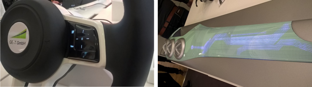
LED foils are one visible example of printed electronics. Using these in large-area structures, designers can create shapes, surfaces, and structures beyond traditional limitations. Manufacturing can be done efficiently and with great speed using roll-to-roll methods [9].
Health technology takes advantage of the opportunities offered by printed intelligence. Among other things, the development of rapid diagnostics test platforms, such as glucose monitoring test strips, is a huge business and still growing rapidly [8]. Wearable devices with integrated printed sensors and electrodes can measure body functions, health, and well-being. The most common examples are printed electrodes in ECG (electrocardiography) or brain activity monitoring, but also wearables are available for measurements of acceleration, elongation, or pressure of the body. When talking about textiles with components integrated by printing methods, the term ”smart clothes” is used. Designer clothing companies have also developed special products taking advantage of the opportunities offered by printed electronics. [10]
More information on current and future application areas will be given in the next articles.

An innovative approach to conventional technology
Manufacturing electronics with functional materials using printing technologies require a lot of development work and practical testing. Specific, suitable equipment and a laboratory environment are other necessities. The rest of the technological development depends on an innovative approach of skillful personnel. Once you are familiar with the restrictions and limitations and the huge potential of the functional materials and technologies available, the world of printed electronics opens its business potential and usability to change the traditional way of manufacturing electronics.
Products utilizing printed technology are already used in several different fields, from components to design elements. Networking among researchers, designers, engineers, and other experts is important for the development of this relatively new field of technology. Innovative ideas, a lot of curiosity, work in practice, and patience are needed to expand into this evolving technology. The development of functional materials, their application to conventional additive printing methods, and the integration of technology into different products and application areas require broad multidisciplinary expertise.
This article is a starting point to a journey through the interesting world of printed intelligence, see you in later articles!
Harri Määttä
Lecturer
Oulu University of Applied Sciences, Information technology
Tomi Tuomaala
Researcher
Oulu University of Applied Sciences, Information technology
Niina Torniainen
Researcher
Oulu University of Applied Sciences, Information technology
Marja Nissinen
Senior Researcher
Oulu University of Applied Sciences, Information technology
References
[1] University of Twente. Functional materials. Accessed 7.11.2022. https://www.utwente.nl/en/max-planck-center/research/Functional/
[2] PrintoCent. 2019. Introduction to Printed Intelligence – Handbook for technology training and coaching.
[3] New Cable Corporation. 2021. How this is possible. Accessed 2.11.2022. https://newcablecorporation.com/technology/
[4] PST Sensors. 2017. Homepage. Accessed 6.6.2022. https://www.pstsensors.com
[5] Brewer Science. 2022. Environmental monitoring through brewer science sensor solutions. Accessed 6.6.2022. https://www.brewerscience.com/products/environmental-monitoring/
[6] Interlink Electronics. 2022. Technologies. Accessed 6.6.2022. https://www.interlinkelectronics.com/sensor-technologies
[7] PARC. 2022. Printed Gas Sensors. Accessed 6.6.2022. https://www.parc.com/information-sheets/printed-gas-sensors/
[8] Singh, S., Wang, J. & Cinti, S. 2022. An Overview on Recent Progress in Screen-Printed Electroanalytical (Bio)Sensors. ECS Sensors Plus 1 (2), 023401. Accessed 24.11.2022. https://doi.org/10.1149/2754-2726/ac70e2
[9] Määttä, H. 2020. R2R printing – a short video introduction. ePooki. Oulun ammattikorkeakoulun tutkimus- ja kehitystyön julkaisut 54. Accessed 6.6.2022. http://urn.fi/urn:isbn:978-951-597-195-1
[10] Tuomaala, T. & Määttä, H. 2019. Painetulla älyllä uusia mahdollisuuksia perinteisen elektroniikan rinnalle. In Paldanius, M. (toim.) Oulun alueen ja Pohjois-Suomen kehitystä tuetaan monipuolisella tutkimus-, kehitys- ja innovaatiotyöllä. ePooki. Oulun ammattikorkeakoulun tutkimus- ja kehitystyön julkaisut 89. Accessed 2.11.2022. http://urn.fi/urn:nbn:fi-fe2019110536728

Vastaa
Sinun täytyy kirjautua sisään kommentoidaksesi.